Construction of Solar Cell: Step-by-Step Guide
When you consider the construction of a solar cell, you’re looking at a complex yet fascinating process that transforms sunlight into electricity. It starts with layering p-type and n-type silicon, creating an essential p-n junction. This is where doping techniques come into play, adding impurities like boron and phosphorus to enhance performance. But have you thought about how anti-reflective coatings and advanced materials boost efficiency further? And what about the encapsulation process that guarantees durability? Understanding these steps could change how you view renewable energy solutions. What makes you curious about how these components work together?
Key Takeaways
- Solar cells are constructed using p-type and n-type silicon layers forming a p-n junction for electricity generation.
- Anti-reflective coatings and advanced materials enhance solar cell efficiency by reducing reflection and increasing light absorption.
- Electrical contacts, typically silver, and aluminum, are integrated to minimize shading and improve current collection.
- Doping techniques introduce impurities to silicon, creating p-type and n-type semiconductors essential for the electric field.
- The encapsulation process involves EVA and tempered glass to protect solar cells from environmental damage and ensure durability.
Definition and Purpose
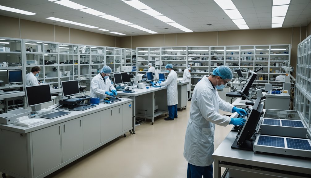
When understanding solar cells, it’s important to know they’re devices designed to convert light into electricity using the photovoltaic effect. A solar cell is made to harness this effect by transforming energy from sunlight into electrical energy.
This conversion process is achieved through a clever design that involves a p-n junction diode. Fundamentally, you have two layers of silicon working together: a thin layer of p-type silicon and a thicker layer of n-type silicon. The p-type silicon is rich in holes, while the n-type silicon has excess electrons.
As sunlight hits the solar cell, it excites electrons, creating electron-hole pairs. This movement of electrons across the silicon layers generates direct current (DC) electricity. The individual solar cells usually produce an open-circuit voltage ranging from 0.5 to 0.6 volts.
Combining them into larger modules can greatly increase the energy output, making solar cells suitable for various applications, from powering small gadgets to forming large solar panels.
Solar cells generate electricity sustainably, providing a renewable energy source contributing to a greener planet.
Key Components
It’s important to explore solar cells’ key components to understand how they function truly. The substrate layer, usually composed of silicon, is at the heart of every solar cell. This layer provides mechanical support and significantly affects the cell’s efficiency.
Silicon is a semiconductor used in two forms: p-type, which has a deficiency of electrons, and n-type, which has an excess. When these two types are combined, they form a p-n junction, the essential element for generating electricity. This junction creates an electric field, enabling the cell to convert sunlight into electrical energy.
Fine metal electrical contacts, often made from silver, are strategically designed to minimize shading while maximizing current collection on the solar cell’s front. These contacts guarantee effective conductivity, which is crucial for the cell’s performance.
Meanwhile, on the back, aluminum electrical contacts efficiently capture and transfer the generated current. This back contact is integral to the photovoltaic module‘s overall efficiency.
The structure is laminated with protective layers, including an encapsulating polymer like ethylene-vinyl acetate (EVA) and tempered glass, safeguarding the cell against environmental elements and mechanical stress.
Semiconductor Layer Formation

When forming the semiconductor layers of a solar cell, you’ll create a p-n junction by doping silicon with specific elements.
P-type silicon is made by adding boron or gallium, introducing electron vacancies, while phosphorus doping gives n-type silicon extra electrons.
This doping process is essential, as it establishes the electric field necessary for charge separation and electric current generation when light hits the solar cell.
P-N Junction Creation
Forming the p-n junction is vital in determining a solar cell’s efficiency and performance. At its core, this junction involves silicon, which acts as the semiconductor where charge carriers are manipulated.
You start by creating two types of silicon: p-type and n-type. You introduce boron or gallium into silicon to achieve this, resulting in p-type silicon with plenty of holes. For n-type silicon, phosphorus is added, contributing extra electrons for conduction.
When these two types of silicon come together, they form the p-n junction. Here, a depletion zone emerges, where free electrons from the n-type layer and holes from the p-type layer recombine. This recombination sets up an internal electric field essential for the movement of charge carriers.
When sunlight strikes the cell, this electric field directs energized electrons toward the n-type layer and holes toward the p-type layer, facilitating charge separation.
The efficiency of this process hinges on the quality of the silicon. Impurities and defects can interfere with electron mobility and recombination rates, affecting the solar cell’s open-circuit voltage, which typically ranges from 0.5 to 0.6 volts for single-junction silicon cells.
Doping Process Essentials
Understanding the doping process is essential for forming the semiconductor layers that power solar cells. Adding specific impurities to silicon creates p-type and n-type semiconductors, vital for establishing the p-n junction. This junction is the heart of a solar cell, where sunlight is converted into electricity. In p-type silicon, boron is added, creating a deficiency of electrons known as holes. Conversely, n-type silicon is formed by adding phosphorus, which supplies excess electrons. This difference in charge carriers enhances electrical conductivity, allowing solar cells to convert light into electrical energy efficiently.
The concentration of these dopants greatly impacts the solar cell’s performance. Typical doping levels range from 1×10^15 to 1×10^19 atoms/cm³. You can use ion implantation or diffusion to introduce dopants into the silicon wafer, ensuring a uniform distribution of charge carriers. The quality of this process directly affects charge carrier mobility and lifetime, which are vital for optimizing performance.
| Doping Type | Impurity Added |
|---|---|
| P-Type | Boron |
| N-Type | Phosphorus |
| Doping Level | 1×10^15 to 1×10^19 atoms/cm³ |
Doping Techniques
When developing doping techniques for solar cells, you will focus on introducing impurities to create p-type and n-type semiconductors.
Adding elements like boron for p-type and phosphorus for n-type enhances the semiconductor properties vital for forming the essential p-n junction.
This precise introduction of impurities, often controlled through advanced methods like ion implantation, greatly boosts the efficiency and performance of your solar cells.
P-Type and N-Type Doping
To truly grasp the intricacies of solar cell construction, you need to understand the vital role of p-type and n-type doping. P-type doping involves adding elements like boron or gallium to silicon, creating holes or electron vacancies. These vacancies act as positive charge carriers, essential for the semiconductor’s performance.
On the other hand, n-type doping is done by introducing phosphorus into silicon. This process provides extra electrons, serving as negative charge carriers and enhancing the material’s electrical conductivity. Together, these doping methods form the essential p-n junction. This junction establishes an internal electric field that separates charges, enabling electricity generation in solar cells.
The doping concentration, typically ranging from 1 x 10^14 to 1 x 10^20 atoms per cubic centimeter, plays a significant role in determining the electrical properties and performance of the solar cell.
Advanced techniques, such as ion implantation and diffusion, precisely control the doping levels and distribution. These methods help optimize the efficiency of the resulting solar cells by ensuring the right balance and interaction between p-type and n-type regions.
Semiconductor Properties Enhancement
Enhancing semiconductor properties through effective doping techniques is vital for optimizing solar cell performance. You can achieve this by introducing impurities into silicon and creating p-type and n-type silicon. For p-type silicon, you’ll use dopants like boron or gallium, which introduce electron vacancies, known as holes. These holes facilitate the flow of positive charge.
On the other hand, n-type silicon is created using phosphorus, which provides excess electrons and enhances electron flow.
The doping concentration is essential because it directly affects charge carrier mobility and helps reduce recombination losses. Properly optimized doping levels guarantee that charge carriers move efficiently, improving the solar cell’s efficiency.
Various doping techniques can achieve this, such as diffusion implantation and vapor deposition. Each method influences how uniformly and deeply the dopant is integrated into the silicon structure.
Exploring advanced methods, like low-temperature or selective doping, can further boost the performance of photovoltaic cells. These innovative approaches aim to refine charge carrier mobility and energy conversion, paving the way for efficient and powerful solar cells in the future.
Layer Deposition Methods

Layer deposition methods like Chemical Vapor Deposition (CVD) and Physical Vapor Deposition (PVD) fundamentally enhance solar cell performance. These techniques are imperative for forming thin semiconductor layers, essential to solar cell efficiency.
With CVD, you can uniformly deposit materials such as silicon, achieving high purity levels critical for efficient charge carrier mobility. This precision guarantees the layers are thin yet effective, optimizing light absorption and electrical conductivity.
PVD, on the other hand, involves methods like sputtering, where material is physically removed from a target to create thin films. This method often deposits metal contacts or anti-reflective coatings on solar cells. Controlling the thickness of these layers, usually in the nanometer to micrometer range, is crucial for maximizing the cell’s overall performance.
As you investigate solar cell manufacturing, understanding these deposition methods is fundamental to developing next-generation technologies that push the boundaries of efficiency and effectiveness.
Electrical Contact Integration
Silver is the best choice for the front contact, forming a fine metal grid that minimizes shading while maximizing conductivity. This grid acts as the current-collecting electrode, significantly affecting the solar cell’s electrical characteristics. On the other hand, aluminum takes the back seat as a full-surface layer, enhancing the electrical connection and durability of the cell.
Proper application of these contacts is essential. Any missteps here can increase resistance, cutting down on overall module efficiency. To paint a clearer picture, here’s how the roles of these materials are distributed:
| Component | Material | Function |
|---|---|---|
| Front Contact | Silver | High conductivity, minimal shading |
| Back Contact | Aluminum | Full-surface connection, durability |
| Current Collecting | Electrode | Efficient current extraction |
Quality monitoring is your best friend during manufacturing. It guarantees the solar cells’ reliability and longevity, directly impacting their performance in real-world applications. Keep the electrical characteristics in check, and your solar cells will perform at their best.
Encapsulation Process
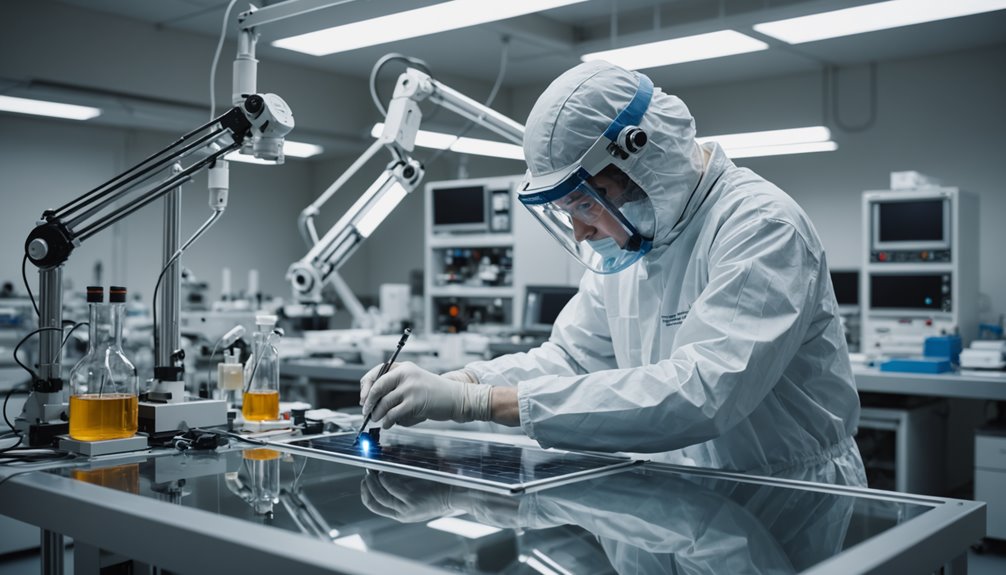
Encapsulation protects solar cells from environmental hazards like moisture, dust, and mechanical stress.
The next step is to apply heat and pressure during lamination. This ensures that the EVA securely bonds to both the cells and the glass, forming a durable protective layer that will withstand the test of time.
Encapsulating solar cells protects them and boosts their performance. This process minimizes the risk of delamination and degradation over time, which are common issues that can compromise efficiency. Adding a polymer back sheet on the rear side of the solar module further enhances protection and provides electrical insulation.
The quality of your encapsulation work will directly impact the longevity and efficiency of the solar panels. A well-executed lamination process can lead to a solar panel lifespan of 25 years or more, guaranteeing a reliable and high-performing energy solution.
Don’t underestimate the power of proper encapsulation!
Efficiency Optimization Strategies
As you investigate efficiency optimization strategies for solar cells, focus on techniques that maximize light absorption and electron mobility tare crucially. Start by considering anti-reflective coatings, which can reduce reflection losses by up to 4% of the incident sunlight, directly boosting cell efficiency. Advanced materials like perovskite and tandem cells enable you to exceed 30% efficiency by stacking layers to capture a broader solar spectrum. To further optimize and enhance electron mobility by doping silicon with elements like phosphorus or boron, which reduces recombination losses and improves the cell’s electric fielding bifacial solar technology, it can also enhance efficiency. By capturing sunlight on both sides of the panel, you can increase total energy output by 10-20%, depending on installation conditions. Additionally, adopting heterojunction technology that combines crystalline silicon with thin-film layers can achieve up to 26% efficiency, offering better performance across various temperatures.
| Strategy | Impact on Cell Efficiency | % Efficiency Improvement |
|---|---|---|
| Anti-reflective coatings | Reduces reflection losses | Up to 4% |
| Bifacial technology | Increases energy capture | 10-20% |
| Heterojunction technology | Enhances temperature range | Up to 26% |
Conclusion
In building solar cells, you create a powerhouse of renewable energy by skillfully layering p-type and n-type silicon. Enhance the semiconductor’s capabilities by precisely doping with boron and phosphorus—guarantee peak performance by carefully depositing layers and integrating electrical contacts. Protect and extend their lifespan by encapsulating the cells with ethylene-vinyl acetate and tempered glass. With these efforts, you’re not just making solar cells but driving a sustainable energy future.
FAQs
1. How Are Solar Cells Constructed?
You construct solar cells using photovoltaic technology, focusing on material selection for maximum efficiency improvement. Start with high-purity silicon, create p-n junctions, and add electrodes. Finally, encapsulate them to protect them from environmental damage.
2. How Do You Make a Solar Cell?
You start by selecting photovoltaic materials, primarily silicon wafers, essential for energy conversion. Next, a p-n junction is created by doping and encapsulating the assembly. This process efficiently transforms sunlight into usable electricity.y
3. How Many Layers Does the Solar CellHave?
Solar cells have up to five layers, including silicon for conductivity, metal grids, and aluminum for support. Anti-reflective coatings are important. Material selection varies with design and technology advancements.
4. How Are Solar Panels Made Step by Step?
You’re learning how to make solar panels step by step. Start with silicon, dope it for photovoltaic efficiency, add semiconductor layers, laminate for solar energy capture, and frame it. Ensure quality before installation to embrace renewable technology.