Exploring the Functionality of AND Gate in Digital Circuits
An AND gate can be considered a sentinel, standing watch in a world of electronic currents. Its role is simple but indispensable, allowing high signals through only when all its inputs are high. It’s like a strict guard that only opens the gate when all group members have arrived. However, if a single input arrives at a low dip, it sends out a low signal, operating on a strict ‘all or none’ code. With this understanding, we begin our journey into the fascinating world of digital circuits.
An AND gate is a fundamental digital logic gate that produces a high output (1) only when all its inputs are high (1). It performs logical conjunction operations and is essential in constructing complex logic circuits for tasks such as arithmetic, data processing, and control functions in electronic devices.
Essentials of the AND Gate
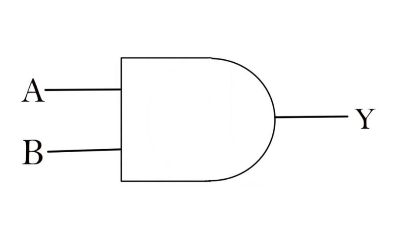
The AND gate is a crucial electronic component in digital systems, responsible for producing an output of logic 1 only when all inputs are at logic level 1. In other words, any low input will give a low output. This behavior is depicted by the word “AND” enclosed within a circle in its symbolic representation.
In practical terms, the AND gate facilitates logical operations where multiple binary signals need simultaneous assessment. It’s akin to requiring all keys to unlock a safe; without each one, it remains securely shut.
The truth table for an AND gate further validates its operation.
Truth Table for an AND Gate
| Input A | Input B | Output |
| 0 | 0 | 0 |
| 0 | 1 | 0 |
| 1 | 0 | 0 |
| 1 | 1 | 1 |
The truth table illustrates the condition necessary for the output to assume a high state: only when inputs A and B are at logic ‘1’ does the output become logic ‘1’. Any other combination results in a low output.
Now that we’ve thoroughly explored the essential function of the AND gate and its operational insights, it’s time to delve into its pivotal role in performing logical operations within digital systems.
Exploring Operational Dynamics of AND Gate
To comprehend the operational dynamics of an AND gate, we can turn to the principles of Boolean algebra. This type of math deals with concepts like “true” and “false,” forming the backbone of digital logic, hinging on the combination of input states.
When we refer to ‘input states’, we’re talking about two specific signals: A and B. These signals can be ‘true’ (or ‘1’ in binary) or ‘false’ (0). The AND gate operates uniquely by producing only a ‘true’ output when both A and B are ‘true’.
Let’s break it down into a simple table to illustrate:
| Input A | Input B | Output Q |
| 0 | 0 | 0 |
| 0 | 1 | 0 |
| 1 | 0 | 0 |
| 1 | 1 | 1 |
In summary, using Boolean algebra, if either A or B (or both) is in a ‘false’ state, the output will also be in a ‘false’ state. Only when A and B are in a ‘true’ state does the AND gate produce a ‘true’ output.
This stringent condition for output generation underscores the importance of AND gates in digital circuitry, particularly in logical decision-making processes. They mimic our everyday if-then thought process — if both conditions are met, then take action. This simple logic forms the basis for more complex calculations and decision pathways in electronic devices and systems.
Understanding these operational dynamics provides insights into how AND gates contribute to the precision and reliability of digital circuits, offering valuable knowledge about their role in logical operations.
Having explored the operational dynamics of AND gates, we can now focus on delving deeper into their role within electronic circuitry.
Electronic Circuitry and the AND Gate’s Role
Imagine the AND gate as a sentinel—it stands guard at the entrance of a digital circuit and permits entrance only to the select few who meet its stringent criteria. Semiconductor devices such as transistors and diodes, which form the building blocks of modern technology, achieve this through the magic of orchestrating complex operations with speed and precision.
Within electronic circuitry, transistors play a starring role. The series connection of transistors within an AND gate is akin to a relay race where each runner must press on to pass the baton forward. Similarly, the inputs to the AND gate must be “active” to produce an output. Visualize it as a traffic light: all signals must be green for the car (or input signal) to move forward. When any signal stays red (i.e., logic level ‘0’), it doesn’t advance. This multiplication of signals within the AND gate exemplifies its innate purpose—to enact an “and” logic operation. In layman’s terms, both input signals must be active for the output signal to mirror their state. The gate’s output remains inactive if either or both inputs are inactive.
Understanding through a Scenario
Consider an everyday scenario: For someone to access your private property, they need a valid ID card and a unique password. If either one is absent, entry is denied. This analogy mirrors the operation of an AND gate in a digital circuit, where access—symbolized by the output—is granted only if both conditions are met. This distinctive functionality forms the bedrock of digital systems and microprocessors, commanding their operation at every level.
Understanding this pivotal role empowers engineers and designers to craft intricate circuits with unwavering precision, ensuring seamless integration amid countless intricate components.
By understanding these complex semiconductor-based activities, you’re well-equipped to harness the full potential of these essential electronic elements in your work.
Mastering the intricacies of AND gates serves as a springboard to their applications within computer microprocessors.
AND Gate Applications in Computer Microprocessors
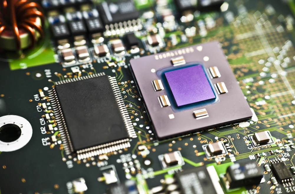
Microprocessors power everything from smartphones to supercomputers. At the core of these microprocessors, many AND gates quietly perform critical tasks, enabling the processor to handle a wide range of operations with precision and speed, making them essential for the efficient function of digital devices.
Data Validation
One fundamental application of AND gates in microprocessors is data validation. When the microprocessor receives data, it must check for accuracy before further processing. This is where the AND gate comes in, functioning as a gatekeeper that verifies whether specific conditions are met before allowing the data to proceed. By utilizing AND gates, the microprocessor ensures that it processes only valid data, contributing to the overall reliability and integrity of the system.
Address Decoding
Address decoding is another critical task that relies on the functionality of AND gates within microprocessors. As a part of this process, the microprocessor employs AND gates to interpret memory addresses and determine which memory location should be accessed. This operation is crucial for the seamless execution of instructions and efficient utilization of memory resources within the digital device.
Role in Arithmetic Functions
Furthermore, when handling arithmetic functions, AND gates play an integral role in microprocessor operations—comparing two values, enabling specific operations based on conditions, or executing logical operations such as bit-wise ANDing. The reliability and efficiency of AND gates are indispensable in ensuring microprocessors perform their tasks effectively and accurately.
Regarding complex mathematical calculations and logical decision-making, the reliability and efficiency afforded by AND gates are indispensable in ensuring microprocessors perform their tasks effectively and accurately.
Microprocessor Operational Functionality
In essence, AND gates form the backbone of a microprocessor’s operational functionality. Their ability to process input signals and generate precise output based on logical conditions underpins modern digital devices’ dependable and efficient performance. Without these small yet powerful electronic components, our digital world could not operate with such speed and accuracy.
In understanding how AND gates function in computer microprocessors, we can now proceed to a practical exploration of building an AND gate circuit.
Practical Guide: Building an AND Gate Circuit
Building an AND gate circuit may initially appear complex, but it becomes much more approachable once you break it down. The first thing to understand is that gates are fundamental for processing binary data in digital logic. They take two input signals and produce an output signal dependent on both true input signals. Let’s take a hands-on approach to understand the functionality and implementation of AND gate circuits.
The key to building an effective AND gate circuit is choosing the right integrated circuit (IC) based on the number of input signals required. For instance, you can easily implement a common 2-input AND gate using a standard IC like the 74LS08. The internal structure of this IC is designed to execute logical conjunction operations, making it an ideal choice for creating simple AND gate circuits.
Connecting the Inputs and Outputs
The cathode would be connected to the input conditions when setting up the IC, while the anode represents the output. This connection plays a pivotal role in defining how the inputs interact with each other and produce an output based on their logical combination.
For instance, imagine a scenario where you want to design a circuit that turns on a light only when both a motion sensor and a temperature sensor detect activity. In this case, you would use an AND gate circuit with two inputs – one from the motion sensor and one from the temperature sensor – and one output connected to the light.
This hands-on design process greatly helps engineers understand how digital circuits execute logical operations, providing valuable insight into theoretical and practical applications.
Ensuring your connections are secure and accurate is essential for the proper functioning of the AND gate circuit. The meticulous nature of connecting these components serves as a practical exercise that reinforces learning and understanding of digital logic principles.
Engineers gain a deeper understanding of their functionality and applications within digital systems by taking a practical, hands-on approach to creating AND gate circuits. This enables them to grasp concepts more effectively and apply them precisely in real-world scenarios.
In preparation for more in-depth insights into digital circuitry, consider evaluating the advantages and constraints associated with AND gate implementations.
Analyzing the Advantages and Constraints of AND Gates

Understanding the advantages and constraints of AND gates is crucial for anyone working with digital circuits. Let’s start by highlighting the advantages.
Advantages
Advantages of AND Gates:
- Logical Operations: The most obvious advantage of AND gates is their ability to perform logical operations. They only produce a high output when both inputs are high, making them crucial for carrying out specific functions in digital systems. It’s like having a lock that requires two keys to be turned simultaneously to open.
- Complexity in Circuits: Another advantage is how AND gates contribute to building complex circuits. By combining multiple AND gates, engineers can create intricate logic networks that form the basis of various digital systems. Think of it like building a puzzle—you need different pieces (AND gates) to form a complete picture (complex digital system).
- Enable Diverse Applications: AND gates enable diverse applications within digital systems, from simple household devices to complex computer processors. They act as the building blocks for logical decision-making, data processing, and controlling electronic devices.
In a traffic light system, an AND gate could ensure that the green signal and the pedestrian crossing symbol illuminate before allowing a car to pass through an intersection. This simple representation illustrates how AND gates enable precise control over interconnected systems.
Constraints
However, despite these valuable advantages, users must consider some constraints when incorporating large AND gates in complex digital circuits.
Constraints of AND Gates:
- Propagation Delay: As more AND gates are cascaded together in larger-scale circuit designs, they contribute to increased propagation delay—the time taken for a signal change at the input of a gate to result in a signal change at the output. This delay can affect the overall performance and speed of a digital system.
- Power Consumption: Besides propagation delay, cascading multiple AND gates increases power consumption. Each additional gate requires more energy to function, which can affect the efficiency and sustainability of digital systems.
Understanding these trade-offs between advantages and constraints empowers engineers to make informed design choices when implementing AND gates within digital systems, balancing functionality with operational performance.
For in-depth insights into logical gates’ functionality and practical applications, visit mytechinfo. Discover how these fundamental components are critical in shaping modern digital technology.