Understanding the Principle Operations of Transistor
Principle Operation of P-N-P Transistor
The basic connection of a p-n-p transistor is shown in the figure below.
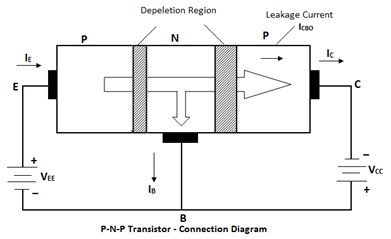
Let us consider the principle operation of transistor action at the emitter-base junction. It is forward-biased, and when the collector is left floating, the majority of carriers (holes) from the emitter diffuse into the base, and the majority of carriers (electrons) from the base diffuse into the emitter.
Now, if the base-collector is reverse biased and the emitter is left floating, then the width of the depletion layer at the base-collector junction increases; hence, there is no flow of majority carriers. However, there is a flow of current due to thermally generated minority carriers.
Now consider the action of a p-n-p transistor whose emitter-base junction is forward-biased and collector–base junction is reverse-biased. Many majority carriers (holes, say, X in the emitter and the electrons, Y in the base will diffuse across the forward-biased p-n junction.
Hence, the total current flowing across this junction is the sum of the hole diffusion current and electron diffusion current. This total current is called the emitter current, denoted by IE,
Emitter Current IE= IP(x) + In(Y)
Since the central region, i.e., the base, is very thin and lightly doped, most carriers that start from the emitter have little chance to recombine in the base and across the base region to reach the collector. Only a few majority carriers (x) are lost due to recombination. In practice, about 2 per cent of the majority carries, which diffuses into the base and recombines with electrons.
The total loss of the number of electrons (Y+y) is the flow of an equal number of electrons from the negative terminal of a DC battery VEE into the base. The base by such electrons constitutes the base current IB. Hence, the magnitude of the base current, IB, is very small and is in the order of micro-amperes.
If X(=y) is the number of holes that combine with the electrons, then the loss of the total number of holes in the emitter is (X+x). This loss comprises the flow of an equal number of electrons from the emitter to the positive terminal of the DC battery VEE. These electrons go from the emitter to the positive terminal of the DC battery VEE. These electrons are released from the covalent bonds of the crystal atoms in the emitter, and an equal number of holes are created.
The potential VCC in the right-hand section is such that the carriers reaching that section get easily attracted as the current starts flowing. This current is called the collector current Ic, almost equal to the emitter current.
The collector current also has a second component of current. This current is due to minority carriers called reverse saturation current; ICBO flows through a reverse-biased collector diode. Hence, the collector current, IC, is the sum of the leakage current, ICBO, and remaining emitter current [=IE(X-y)]
= IC(X-y) + ICBO
The larger the number of carriers reaching the collector from the emitter, the larger the power gain of the device. The base should be very thin, and the collector–base junction area should be large. So, the collector current is only slightly higher than the emitter current.
Applying Kirchoff’s current law to the transistor, we get,
Principle Operation of N-P-N Transistor
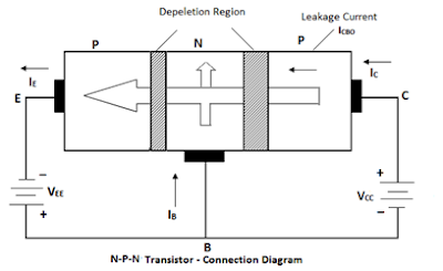
The figure above shows the n-p-n transistor with a forward bias to the emitter-base junction and a reverse bias to the collector-base junction. The forward bias VEE causes the majority carriers (electrons) in the n-type emitter to diffuse into the base, and holes from the base diffuse into the emitter.
The flow of majority carries constitutes the emitter current. As these electrons flow through the p-type base, they tend to combine with holes. Only a few combine with holes as the base is lightly doped and thin. As the base is slightly doped and thin, only a few electrons combine with holes to form base current IB.
The remaining electrons cross into the collector region to constitute the current IC. This collector current is also called injected current because it is produced by electrons injected from the emitter region.
The emitter current is the sum of the collector current and base current.
Points to remember
-
The emitter current of a transistor consists of two components: base current and collector current.
-
The base current is a small fraction of the emitter current, i.e., about 2% of the emitter current, and the collector current is about 98%.
-
The collector current is mainly due to injected electrons (majority carriers) from the emitter. The collector current also has a second component due to thermally generated minority carriers, called reverse saturation current.
-
The emitter-base junction is always forward-biased, and the collector-base junction is reverse-biased.
Conclusion
In conclusion, the operation of P-N-P and N-P-N transistors is at the core of electronic circuitry. These devices enable us to control and amplify electrical signals, making them indispensable in modern technology. Whether it’s amplifying audio signals in your headphones or processing data in your computer, transistors are the unsung heroes of the digital age. By grasping the principles outlined in this article, you can better appreciate the magic happening inside your electronic devices.
FAQs
What is the main difference between P-N-P and N-P-N transistors?
The primary difference lies in the semiconductor materials used in their construction. P-N-P transistors use P-type material for the emitter and collector, while N-P-N transistors use N-type material for these regions.
Why is the base current in transistors so small?
The base current is intentionally kept small to ensure that most majority carriers (electrons or holes) from the emitter flow into the collector, allowing for amplification. Only a small fraction of these carriers form the base current.
What causes the collector current in a transistor?
The collector current consists mainly of electrons injected from the emitter, most carriers. Additionally, there is a smaller component called the reverse saturation current, resulting from thermally generated minority carriers in the collector-base junction.