Unveiling Potential of Transistors in Common Base Configuration
The common base configuration of an n-p-n transistor is a fundamental electronic circuit arrangement with significant implications for amplifier design and transistor theory. In this setup, the emitter current is the input, and the collector current is the output. Engineers and electronics enthusiasts must understand its characteristics, such as the current amplification factor (α) and the relationship between IC and IE. In this article, we explore the key aspects of the common base configuration without altering the established equations and patterns.
Common Base Configuration
Consider an n-p-n transistor in a common base configuration. In this common base configuration, emitter current IE is the input, and collector current IC is the output current.
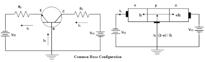
Current Amplification Factor (α)
The ratio of the transistor’s output current to the input current is known as the current gain of a transistor. Specifically, the ratio of the collector current to the emitter current is referred to as the DC forward current transfer ratio or DC gain, denoted as αdc.
Common Base DC Current Gain, αdc = IC / IE.
IC and IE represent the magnitudes of the collector and emitter currents at a specific point on the transistor’s characteristics. Since the collector current is always less than the emitter current, αdc is always less than unity. Typical values of αdc typically range from 0.95 to 0.998.
From the equation αdc = IC / IE, we can express IC as IC = αdc IE.
Simplifying further, if we write αdc simply as α, IC = αIE.
Since IC = IC(majority) + ICBO(minority), we can rewrite the equation as:
IC = α IC (majority) + ICBO
We also know that IE = IC + IB or IB = IE – IC = IE – (αIE + ICBO),
which can be further simplified as:
IB = IE (1-α) – ICBO
Neglecting ICBO, we can write IB = IE (1-α).
Common-Base Short Circuit (AC) Current Gain
Common-Base Short Circuit (AC) Current Gain is defined as the ratio of a small change in collector current (ΔIC) to the corresponding shift in emitter current (ΔIE) at constant collector-base voltage. It is denoted by αac.
αac = (ΔIC / ΔIE) / VCB = constant.
For practical purposes, the DC gain is considered equal to the AC gain, i.e., αdc = αac.
It’s important to note that α is not a constant but varies with emitter current IE, collector-to-base voltage VCB, and temperature.
The current gain of a transistor in a common-base configuration is less than unity due to the output resistance of the common-base transistor being much higher than the input resistance. This results in a large voltage gain and, subsequently, a large power gain.
Characteristics of Common Base Configuration
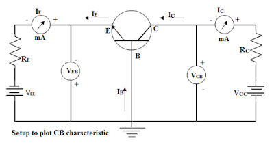
Input Characteristics of common base configuration (VEEvs IE, VCB= Constant)
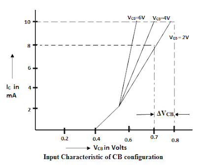
When the collector-to-base voltage VCB is kept constant (e.g., 2V), we vary the emitter-to-base voltage VEB in small steps (e.g., 0.1V increments) and note the corresponding values of emitter current IE for each VEB value. This test is repeated for various VCB values. It’s observed that increasing levels of VCB result in a reduced level of VEB to establish the same current.
The input characteristic of a typical common-base transistor is shown in the figure, with emitter current IE along the Y-axis and emitter-base voltage VEB along the X-axis. Note the tight grouping of the curves over a wide range of VCB values. The average value of the curve starts to rise at approximately VEB = 0.5V for a silicon transistor at 25°C.
Emitter currents are nearly independent of VCB. Similar to a semiconductor silicon diode, a first approximation for the forward-biased base-emitter junction in the DC mode would be VEB = 0.7V.
Output Characteristic of common base configuration (VCBVs IC, IE= Constant)
In this scenario, the emitter current IE is kept constant (e.g., 2mA), while the collector-to-base voltage varies from zero inappropriate steps (e.g., 1V increments). Corresponding values of IC are noted. This experiment is repeated for different values of IE, and the obtained output characteristic curves are illustrated in the figure.

The output characteristics of the common-base configuration can be divided into three distinct regions:
- Active Region: At the right of the line, VCB = 0 and above the emitter current, IE = 0. In this region, the collector current remains constant and is almost equal to the emitter current.
- Saturation Region: Positioned to the left of the line VCB = 0 and above the output characteristic when IE = 0. In this region, the collector current, IC, increases sharply for a small change in VCB. The relationship between IC and IE in the active region is approximated as IC = IE.
- Cut-off Region: IE = 0, and IC = ICBO, representing the leakage current of the collector-base diode.
The characteristic output curve can be used to determine the dynamic output resistance, defined as the ratio of a small change in the collector-to-base voltage to the corresponding shift in collector current at constant emitter current:
Output Resistance (Ro) = {ΔVCB / ΔIC} IE = Constant.
The reciprocal of the slope of the output characteristics provides the dynamic output resistance, which is typically very high and on the order of mega ohms.
Additionally, the characteristic can be used to determine the transistor’s small-signal common-base current gain (αac) by selecting two points, M and N, on the characteristic and noting the corresponding values of ΔIC and ΔIE.
αdc = ΔIC / ΔIE = 2mA / 2mA = 1 mA
These insights into the common-base configuration provide a comprehensive understanding of transistor behaviour in this specific mode.
Conclusion
In conclusion, the common base configuration of a transistor offers valuable insights into transistor behaviour, particularly in terms of current gain and characteristics. The relationship between collector and emitter currents and the impact of collector-to-base voltage and temperature becomes clearer through this analysis. The distinct active, saturation and cut-off regions provide a comprehensive view of transistor operation. The high dynamic output resistance and common-base current gain (αac) further enhance our understanding of this essential electronic circuit.