PN Junction Diode
If a function is formed between a sample of P-type semiconductor and N type semiconductor, and this device called the PN junction or junction diode possess the properties of a rectifier.
Open Circuited PN Junction:
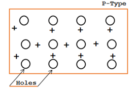
The figure below represents two blocks of semiconductor material, one P type and other N type. In the P type material the small circles represent holes, which are the majority charge carries in that type of material.
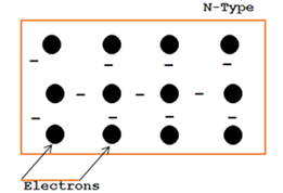
The dots in the N type material represent the majority charge carrier free electrons within that material. Normally the holes are uniformly distributed throughout the volume of the P type, and the electrons are uniformly distributed in the N type semiconductor.
-
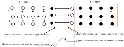
In the above figure P type and N type semiconductor materials are shown side by side, representing a PN junction. Because holes and electrons are close together at the junction, some free electrons from the N side are attached across the junction to fill holes on the P side.
-
They are said to diffuse across junction, i.e. flow from the junction create negative ions on the P side by giving some atoms one more electron than their total number of protons. The electrons also leave positive ions behind them on the N side.
-
When a P type semiconductor is suitably joined to N type semiconductor the contact surface is called PN junction.
Formation of PN Junction
-
The process involved in the formation of a PN junction are summarized below.
-
Holes from the P side diffuse into N side where they combine with free electrons.
-
Free electrons from N side diffuse into the P side where they combine with holes
-
The diffusion current also known as recombination current delays exponentially both with time and distance from the junction.
-
Due to the departure of free and mobile carriers from both sides of the junction, a depletion layer is formed. This layer contains only immobile or fixed ions of opposite polarity.
-
These uncovered by fixed ions setup a potential barrier across the junction.
-
This potential difference opposes the diffusion of free majority charge carriers from one side of the junction to the other till the process is completely stopped.
-
The width of the depletion layer depends on the doping level. For heavy doping, the depletion layer is physically thin because a diffusing charge carrier (either from electron or holes) has not to travel far across the junction for recombination.