Mos Capacitor: Key Components for Efficient Electronics
Imagine you’re uncovering the secrets of the MOS capacitor, a foundational element in modern electronics. It’s a simple yet ingenious structure, consisting of a metal gate, an insulating dielectric, and a semiconductor. This tiny component is pivotal for managing charge distribution, crucial for the operation of MOSFETs and integrated circuits. Its evolution, including the adoption of high-κ dielectrics, has shaped semiconductor technology. Curious about its impact on today’s devices?
Structure and Composition of MOS Capacitors

When examining the structure and composition of MOS capacitors, you’ll find they consist of three main components: a metal gate, an insulating dielectric layer, and a semiconductor body.
The metal gate, usually made of heavily doped n+ poly-silicon, acts as a vital component, serving as the gate terminal. This is separated from the semiconductor substrate by a dielectric layer, typically silicon dioxide (SiO2).
This layer is crucial as it allows the modulation of the electric field when an applied gate voltage is present. The MOS capacitor’s structure impacts the capacitance per unit area, influencing MOS transistors’ performance.
This configuration creates a depletion region in the semiconductor body, which plays a significant role in controlling charge distribution within the channel.
Capacitance and Voltage Dynamics
As you explore the capacitance and voltage dynamics of a MOS capacitor, notice how its capacitance changes with varying gate voltages.
Initially, when the gate voltage surpasses the flatband voltage, positive charges accumulate, increasing capacitance. A negative voltage causes depletion, reducing the semiconductor’s surface charge.
At the flatband voltage, the MOS capacitor’s plates hold no charge, and there’s no electric field across the oxide layer. As you continue to increase the gate voltage, reaching the threshold voltage, the depletion layer disappears.
This critical transition marks the shift from depletion to strong inversion, crucial for transistor operations. The C-V curve of a MOS capacitor vividly illustrates these transitions, highlighting the interplay between accumulation, depletion, and inversion regions.
Historical Development and Impact
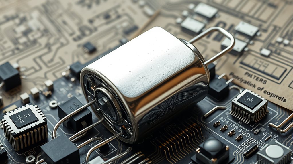
The birth of the Metal-Oxide-Semiconductor (MOS) capacitor in 1960 by Mohamed Atalla and Dawon Kahng at Bell Labs wasn’t just a breakthrough; it revolutionized semiconductor technology.
By introducing the MOS structure, they paved the way for MOS capacitors to become integral in the world of integrated circuits. These capacitors, using silicon and dielectric material, offered low leakage and improved efficiency in handling electronic signals.
The transition from silicon dioxide to high-κ dielectrics further enhanced their performance, reducing power consumption in digital circuits.
Following the first commercial MOS integrated circuit in 1964, the impact of these capacitors became undeniable. They’ve directly influenced advancements across digital and analog circuits, driving innovations in computing, telecommunications, and consumer electronics, shaping the modern technological landscape.
Applications and Technological Significance
Although often overlooked, MOS capacitors are crucial components in modern electronics, underpinning the functionality of MOSFETs across various applications. In digital circuits, they enable precise control of charge distribution, essential for integrated circuits and efficient signal processing.
You’ll find their capacitance-voltage relationship vital for circuit design, allowing you to understand and predict behavior within MOS transistors.
MOS capacitors are key to achieving low power consumption, particularly in CMOS technology. They help create energy-efficient circuits, which is increasingly important as devices become more complex.
Additionally, they play a role in local supply decoupling applications, stabilizing power supply voltages, and enhancing device reliability. Their technological significance in maintaining efficient and reliable integrated circuits can’t be overstated.
Modeling and Design Challenges
When diving into the modeling and design challenges of MOS capacitors, you’ll find that accuracy is paramount. The gate’s voltage applied affects the capacitance, requiring an accurate model to predict performance in integrated circuits.
Layout-dependent effects (LDE) significantly impact this process, making it crucial to account for them. The flat band voltage and threshold voltage are key parameters, defining critical charge states and operational regions.
You’ll also need to manage the depletion layer dynamics carefully. The insulating layer, typically silicon dioxide, demands precise fabrication control to maintain quality and prevent leakage.
Simulation software becomes indispensable, helping you achieve capacitance accuracy and match requirements. By addressing these challenges, you ensure MOS capacitors meet desired performance across varying conditions.
Conclusion
You’ve explored the essential role of MOS capacitors in modern electronics, understanding their structure and how they manage charge distribution. Their evolution, from traditional to high-κ dielectrics, highlights their impact on enhancing device efficiency and performance. These capacitors are pivotal in applications like CMOS, where they help reduce power consumption. As you dive into modeling and design, you’ll face challenges but gain insights crucial for advancing semiconductor technology. Embrace these opportunities to innovate and improve electronic devices.
FAQs
1. What Is a MOS Capacitor?
You’re curious about a MOS capacitor. It’s a device in electronics with a metal gate, insulating oxide, and silicon substrate. It adjusts its capacitance based on voltage, crucial for various circuits, especially in digital and analog systems.
2. What Is the Difference Between a MOSFET and a MOS Capacitor?
You differentiate a MOSFET and a MOS capacitor by their functions. A MOSFET controls current flow in circuits, while a MOS capacitor varies capacitance with gate voltage, affecting charge distribution in the semiconductor. They’re foundational in electronics.
3. What Is the Difference Between Mom Mim and MOS Capacitors?
You’ll find MOM capacitors excel in high-density applications due to interdigitated layers, while MIM capacitors offer high capacitance with parallel plates. MOS capacitors vary in capacitance with voltage, crucial for MOS transistors. Each serves distinct purposes.
4. What Is an Ideal MOS Capacitor?
You’re looking at an ideal capacitor with a metal gate, insulating layer, and semiconductor substrate. The gate voltage influences its capacitance, causing changes like accumulation, depletion, and inversion, and the flat band voltage equals zero electric field.