Intricacies of the Common Emitter Configuration
In this context, “intricacies” refer to the subtle details, complexities, and peculiarities of the common emitter configuration’s design, analysis, and operation. These intricacies encompass areas like load handling, impedance control, response optimization, and the understanding of capacitance and inductance. Furthermore, they shed light on coupling and decoupling techniques and the importance of bypass arrangements. Understanding these facets is crucial for electronics engineers and hobbyists to build efficient and stable amplifiers. Moreover, it aids those studying electronics to comprehend the underlying principles of transistor-based circuits.
Principle of the Common Emitter Configuration
= (IC + IB) + ICBO or
IC (1-α) = αIB + ICBO
IC = [α/(1-α)]IB + ICBO/(1-α)

- A common emitter configuration is a transistor amplifier circuit that uses an n-p-n transistor.
- The base current (IB) is the input current supplied through the base-emitter junction.
- The collector current (IC) is the output current flowing through the collector-emitter junction.
- It provides current amplification, where a small change in IB leads to a larger shift in IC.
- The output signal across the collector-emitter junction is phase-inverted compared to the input signal at the base-emitter junction.
- Proper biasing is essential for stable and linear transistor operation.
- Applications include audio amplifiers, radio frequency circuits, and signal processing circuits, where weak signal amplification is needed.
Common Emitter Configuration
The common emitter configuration is a fundamental transistor amplifier setup widely used in electronic circuits. In this configuration, the emitter terminal is common to both the input and output circuits, while the base and collector terminals serve as the input and output ports, respectively. When a small input voltage is applied to the base terminal, it controls the current flowing between the collector and emitter, amplifying the input signal.
Current Amplification Factor
The ratio of the collector current to the base current is called the DC forward current transfer ratio or the DC gain. It is designated by βdc. It is said to be the dc beta.
Common Emitter DC gain βdc = IC/IB
Where IC and IB are the collector and base current of a particular operating point in the linear region, as the value of base current is in micro amperes and low, the value of βdc lies in the range of 10 to 500 depending on the transistor type.
Common emitter AC gain βdc is the ratio of small change in collector current ΔIB at a constant collector to emitter voltage VCE.
Electric Potential and Potential Difference
Electric potential, also known as voltage, is a fundamental concept in electromagnetism. A scalar quantity describes a given point in an electric field. In simpler terms, it indicates the amount of electric potential energy a positive test charge would possess if placed at that particular point in the electric field.
The electric potential (V) at a point is measured in volts (V). It is calculated as the work done in moving a positive test charge (q) from an infinitely far distance to the point against the electric field, divided by the charge itself:
V=qW
Where:
- V is the electric potential in volts (V).
- W is the work done in joules (J).
- q is the test charge in coulombs (C).
Electric potential is fundamental in understanding electric fields and how charged particles interact.
Potential Difference
The potential difference, or voltage difference or voltage drop, represents an electric field. It is a vector quantity, indicating both the magnitude and direction of the difference in electric potential between the two points.
The potential difference (ΔV or V_ab) between two points’ a’ and ‘b’ is calculated as the change in electric potential energy experienced by a positive test charge (q) as it moves from point’ a’ to point ‘b’:
ΔV=Vb−Va
- V_b is the electric potential at point ‘b’ in volts (V).
- V_a is the electric potential at point ‘a’ in volts (V).
Potential difference is a fundamental concept in electrical circuits as it determines the flow of electric charge (current) from higher potential to lower potential. It is the driving force behind the movement of electrons in a circuit. It is crucial in various electrical applications, including powering electronic devices and generating electric currents in power systems.
Relation between αdc and βdc
Dividing by IC
IE/IC = 1+(IB/IC)
α = β / (β+1) ——> ii
α(β+1) =β
αβ+α =β
α = β – αβ = β (1 – α)
β = α / (α+1) ——-> iiii
α = β / (β+1)
1-α = 1 – [β / (β+1)] ——>iv
From equation (iii), it is seen that as α approaches unity, β approaches infinity.
That is, the current gain of transistors in a common emitter configuration is very high. It is because of this reason that transistors are used in common emitter configurations.
We know that, IC = [αIB / (1-α)] + ICBO / (1-α) —–>v
IC = βIB + (β+1) ICBO ——->vi
ICEO = (β+1)ICBO ——>vii
IC = βIB + ICEO ——->viii
ICEO = [α / (1-α)] ICBO ——->ix
ICEO = ICEO / (1-α )
The leakage current in the common emitter configuration is larger than in the common base configuration. ICE is the collector current that flows when the base-emitter circuit is left open and the collector-base junction is reverse-biased. It is in the same direction as normal collector current flows through the transistor and is temperature-sensitive.
Characteristics of Common Emitter Configuration
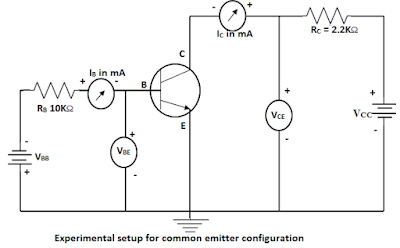
The figure above shows the experimental setup for determining the static characteristic of an n-p-n transistor used in a common emitter configuration circuit. Two variable-regulated power supplies, VBB and VCC, are connected to a transistor’s base and collector terminals.</ >
Input Characteristic (VBEvs IB) VCE= Constant
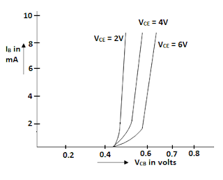
From the input characteristic, we observe the following important points:
-
There exists a threshold, cut in voltage Vγ below which the base current IB is very small. The value of cut-in voltage is 0.5 V for Si and 0.1V for GE transistors.
-
After the cut in voltage, the base current IB increases rapidly with a small increase in base-emitter voltage VBE. However, it may be noted that the value of the base current does not increase as rapidly as that of the input characteristic of a common base configuration. It means that dynamic input resistance is small in the common emitter configuration but slightly higher than in the CB configuration.
-
For a fixed value of VBE, IB increases as VCE is decreased. A large value of VCE results in a larger reverse bias at the collector-base PN junction. This increases the depletion region and reduces the base’s effective width, reducing the base current.
-
Dynamic or AC input resistance can be determined from the input characteristics curve. It is the ratio of a small change in the base-to-emitter voltage to the resulting change in the base current at constant to-emitter voltage.
Input Resistance RO = [ΔVBE/ΔIB] at VCE = constant
Output Characteristics (VCEvs IC) at IB=Constant
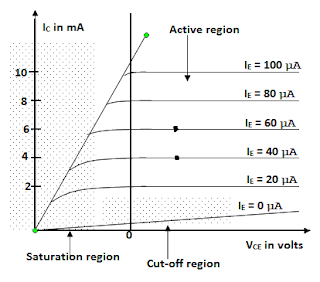
-
The output characteristic of the common emitter configuration curves is obtained by plotting VCE vs. IC for different values of IB. The collector current varies with VCE for values between 0V and 1V. The collector current varies with VCE for values between 0V and 1V. After this collector, the current IC becomes almost constant and reaches the saturation values. The transistors are operated in the region above knee voltage. This region is called the active region. The experiment is repeated for different values of IB.
-
The output characteristics curves may be divided into three regions. They are
-
Saturation region
-
Cut-off region
-
Active region
-
In the above figure, the active region is the area to the right of the ordinate VCE = a few tenths of a voltage and above IB = 0.
-
Ideally, when VCE exceeds 0.7V, the base-collector junction becomes reversely biased, and the transistor goes into its operation’s active or linear region. Once the base-collector junction is reverse biased, IC levels off and remains almost constant for a given value of IB as VCE continues to increase. IC increases very slightly as VCE increases due to the widening of the base-collector depletion region. This phenomenon is called a near effect.
-
When the base current IB is zero, a small collector current exists. This is called leakage current. However, for all practical purposes, the collector current is zero when the base current is zero. Under this condition, the transistor is said to be cut off. The small collector current is called the collector cut-off current.
-
When VCE reaches a sufficiently high voltage, the reverse biased collector junction goes into the breakdown, and therefore, the collector current increases rapidly. If VCE exceeds 40 V, the collector diode breaks down, and normal transistor action is lost. The transistor is not intended to operate in the breakdown region. This effect is commonly known as a punch-through effect.
-
From the output characteristics, the dynamic output resistance can be determined.
Principle of Electronics
Dynamic output resistance Rout = [ΔVCE/ΔIC] at IB = constant
-
The reciprocal of the slope of the output characteristic in the region gives the output resistance. The value of Rout ranges from 10KΩ to 50 KΩ.
-
The output characteristic may be used to determine the small signal common emitter current gain or ac beta (βac) of a transistor. This can be done by selecting the two points M and N on the characteristic and noting the corresponding values of ΔIE and ΔIB.