Decoding the Power of NAND Gates: A Comprehensive Journey
In the ever-evolving landscape of digital electronics, the NAND gate emerges as a cornerstone, weaving its influence through the intricate tapestry of circuit design. This article embarks on a comprehensive journey into the realm of NAND gates, unraveling their symbolic representations, dissecting truth tables, and delving into their applications. From the basics of NAND gate operation to the transistor-level intricacies, this exploration seeks to equip enthusiasts, students, and professionals alike with a profound understanding of this fundamental building block.
What is a NAND Gate?
A NAND gate, short for NOT-AND, is a digital logic gate that performs a negated AND operation. In simpler terms, it produces an output opposite of an AND gate. The output is high (1) only when one or more of its inputs are low (0), making it a versatile component in digital circuit design.
Symbol and Truth Table of NAND Gate
The symbol of a NAND gate is easily recognizable—a triangle pointing to the right with its inputs on the left and the output on the right. The truth table, an essential reference in digital logic, succinctly outlines the output based on the combination of inputs.
NAND Gate Symbol
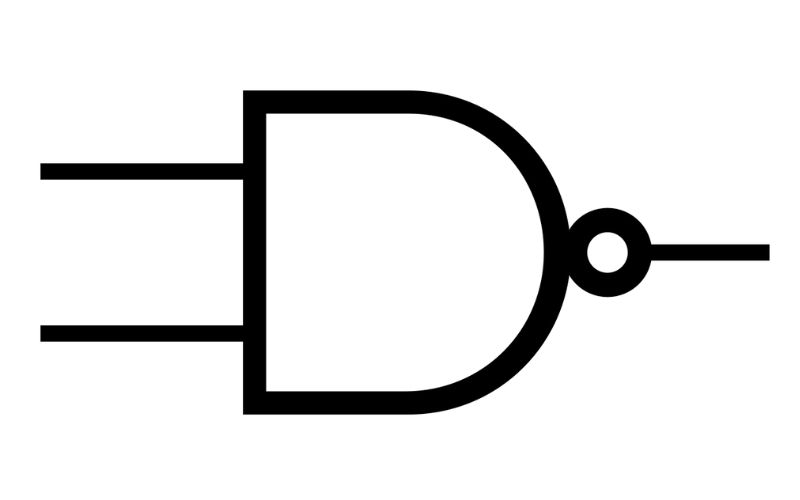
Truth Table
| Input A | Input B | Output |
|---|---|---|
| 0 | 0 | 1 |
| 0 | 1 | 1 |
| 1 | 0 | 1 |
| 1 | 1 | 0 |
The Basics of NAND Gate Operation
The operation of a NAND gate follows a simple rule: it produces a high output only when all of its inputs are low. A NAND gate’s output (Q) is mathematically expressed as Q = NOT(A AND B), where A and B are the inputs.
Understanding this fundamental operation is crucial for more complex circuit designs, as NAND gates are key components in digital systems.
Types of NAND Gates
The two main types of NAND gates, based on the number of inputs, are;
2-Input NAND Gate
The 2-input NAND gate is the most common type, taking two binary inputs and producing a single output. Its truth table is as follows:
| Input A | Input B | Output |
|---|---|---|
| 0 | 0 | 1 |
| 0 | 1 | 1 |
| 1 | 0 | 1 |
| 1 | 1 | 0 |
Timing Diagram for a 2-Input NAND Gate
A visual representation of a timing diagram can aid in understanding the behavior of a NAND gate over time. This graph illustrates the input and output transitions, highlighting the propagation delay and setup/hold times. Refer to the table below:
| Time Step | Input A | Input B | Output |
|---|---|---|---|
| 0 | 0 | 0 | 1 |
| 1 | 0 | 1 | 1 |
| 2 | 1 | 0 | 1 |
| 3 | 1 | 1 | 0 |
3-Input NAND Gate
For more complex scenarios, the 3-input NAND gate is employed. Its truth table expands to accommodate three binary inputs:
| Input A | Input B | Input C | Output |
|---|---|---|---|
| 0 | 0 | 0 | 1 |
| 0 | 0 | 1 | 1 |
| 0 | 1 | 0 | 1 |
| 0 | 1 | 1 | 1 |
| 1 | 0 | 0 | 1 |
| 1 | 0 | 1 | 1 |
| 1 | 1 | 0 | 1 |
| 1 | 1 | 1 | 0 |
Applications of NAND Gate
NAND gates find application in various digital circuits and systems. Some notable applications include:
- Memory Units: NAND gates are essential to constructing memory units, such as RAM and flash memory.
- Arithmetic Logic Units (ALUs): In CPUs, NAND gates play a vital role in ALUs, performing arithmetic and logic operations.
- Digital Signal Processing: NAND gates contribute to the processing of digital signals in various applications, from telecommunications to audio processing.
- Flip-Flops and Latches: These fundamental building blocks of sequential circuits heavily rely on NAND gates.
NAND Gate in Terms of Transistor

Underneath the symbolic representation lies the electronic implementation of NAND gates using transistors. Transistors serve as the building blocks of these gates, enabling the manipulation of electrical signals.
Understanding the transistor-level operation provides insight into the physical realization of NAND gates, a crucial aspect for those diving into the hardware aspects of digital electronics.
Advantages of NAND Gate
NAND gates offer several advantages, making them indispensable in digital circuit design:
- Simplicity: NAND gates are relatively simple to design and implement, contributing to the overall simplicity of digital circuits.
- Universality: NAND gates are universal, meaning any other gate type can be constructed using only NAND gates.
- Versatility: Their versatility in creating various logic functions adds to their appeal in circuit design.
Disadvantages of NAND Gate
While NAND gates are versatile and widely used, they do have some limitations:
- Propagation Delay: NAND gates exhibit a certain propagation delay, affecting signal transmission speed through a circuit.
- Power Consumption: Compared to other gates, NAND gates can consume more power, especially in larger circuits.
- Complexity in Large Circuits: As circuits grow in complexity, managing the interconnections of NAND gates can become challenging.
NAND Gate Flip-Flops and Memory Units

Flip-flops, crucial for storing binary information in digital circuits, are often constructed using NAND gates. The stability and predictability of NAND gates make them ideal for building these memory units. Moreover, NAND gates are the building blocks of flash memory cells, which are prevalent in various storage devices, including USB and solid-state drives.
NAND Gate in Integrated Circuits (ICs)
Beyond individual gate usage, NAND gates are integral to integrated circuits (ICs). Modern ICs often incorporate multiple NAND gates into a single package, streamlining the design and manufacturing process. These ICs find applications in various electronic devices, from smartphones to complex computer systems.
Conclusion
FAQs
1. How does a NAND gate differ from other logic gates?
The NAND gate distinguishes itself by performing a negated AND operation. Unlike its counterpart, the AND gate, the NAND gate produces an output that is only low when all its inputs are high. This unique behavior makes NAND gates essential for certain logic functions and contributes to their widespread use in digital circuit design.
2. Can NAND gates be cascaded to create more complex circuits?
Indeed, the cascading of NAND gates forms the backbone of creating complex digital circuits. Designers can fashion various logic functions and sequential elements by interconnecting multiple NAND gates. This capability underscores the versatility and importance of NAND gates in creating sophisticated digital systems.
3. How do NAND gates contribute to power consumption in electronic devices?
While NAND gates offer simplicity and versatility, they are not without drawbacks. One significant consideration is their impact on power consumption. In larger circuits, where numerous gates are interconnected, the cumulative power consumption of NAND gates can become a factor to be reckoned with. Engineers must balance functionality and power efficiency in their designs to ensure optimal performance.