Transistor Circuit Configuration
Three Transistor Configurations
-
The input is applied between the common terminal and one of the other two terminals. The output is taken between the common terminal and the remaining terminal.
-
The term common denotes the region common to the input and output circuits.
-
Accordingly, a transistor can be connected in the following three different configurations.
Transistor Circuit Configuration
The figure below shows the transistor circuit configuration with n-p-n transistors:
-
Common – Base (CB) connection
-
Common – Emitter (CE) connection
-
Common – Collector (CC) connection
Common – Base (CB) connection
The Common – Base (CB) connection is a fundamental configuration used in bipolar junction transistors (BJTs) in electronics. It involves connecting the base terminal to the common terminal, typically the negative terminal or ground. The emitter terminal is connected to the input signal, while the collector terminal is connected to the output load. Also known as the grounded-base configuration, the CB connection has distinct characteristics and applications. It offers current amplification, where a small change in the recent input results in a larger shift in the output current. However, the voltage gain is less than unity, meaning the output voltage is smaller than the input voltage.
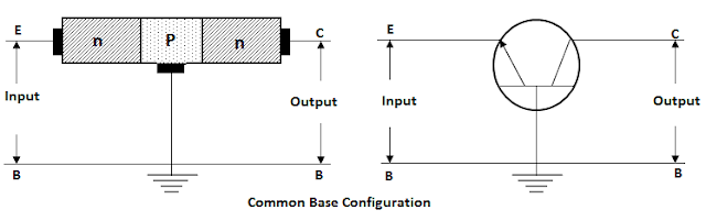
The CB configuration finds use in impedance matching, frequency multiplication, and high-frequency amplification, although it is less commonly employed than other configurations such as Common-Emitter (CE) and Common-Collector (CC). By understanding the CB connection and its unique attributes, engineers can select the appropriate transistor configuration to meet the requirements of their specific circuits or systems.
Common – Emitter (CE) connection
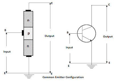
The Common – Emitter (CE) connection is one of the primary configurations used in bipolar junction transistors (BJTs) and holds significant importance in electronics. In this configuration, the emitter terminal is connected to the common terminal or ground, while the base terminal serves as the input and the collector terminal as the output. The CE connection offers several advantages, making it the most widely used configuration. It provides both voltage and current amplification, allowing small changes in the input current to result in larger changes in the output current.
This configuration also offers voltage gain, where the output voltage can be significantly higher than the input voltage. The CE connection has a relatively high input impedance and a low output impedance, making it suitable for various applications, including audio amplifiers, voltage amplifiers, and signal processing circuits. It’s versatility and robust performance have established the CE connection as a fundamental building block in modern electronics.
Common – Collector (CC) connection
The Common – Collector (CC) connection, also known as the emitter follower configuration or the voltage follower configuration, is a basic circuit configuration utilized in bipolar junction transistors (BJTs) in electronics. In this configuration, the collector terminal is connected to the common terminal or ground, while the emitter terminal serves as the output and the base terminal as the input. The CC connection offers unique characteristics and finds widespread use in various applications.
One significant advantage of the CC configuration is that it provides a high input impedance, making it ideal for impedance matching between different stages of a circuit. Additionally, it offers a low output impedance, allowing it to drive low-impedance loads effectively.
The CC connection has a voltage gain slightly less than unity, meaning that the output voltage follows the input voltage closely, resulting in voltage buffering rather than amplification. This feature makes it useful in applications where the primary objective is to maintain signal integrity and provide isolation between the input and output stages.

Moreover, the CC configuration provides excellent current gain, ensuring that the output current tracks the input current with minimal distortion. This property suits impedance bridging, buffering, and signal isolation applications.
Furthermore, the CC configuration exhibits a phase shift of approximately 180 degrees between the input and output signals, which can be advantageous in certain circuits where phase relationships are critical.
Due to its ability to match impedance, low output impedance, and voltage buffering, the CC connection is commonly used in audio amplifiers, buffer stages, and as an interface between different circuit parts. It’s versatile characteristics and wide range of applications make the CC connection vital in modern electronic design.
Biased Transistor
-
Forward active mode
-
saturation mode
-
cut-off mode
Forward Active Mode
Saturation Mode
Cut-off mode
In this mode, both emitter-base junctions and collector-base junctions are reverse-biased. In this case, the current in the transistor is practically zero. The transistor is operated in this mode when it is to be used as an open switch; for the switching application of a transistor, saturation, and cut-off methods are used alternatively.
Comparison of Transistor Configurations
| Common Emitter | Common Collector | Common Base | |
|
Voltage Gain
|
Medium
|
Low
|
High
|
|
Current Gain
|
Medium
|
High
|
Low
|
|
Input Impedance
|
Medium
|
High
|
Low
|
|
Output Impedance
|
Medium
|
Low
|
High
|
Conclusion:
Throughout this article, we have delved into the basic transistor circuit configurations, such as the common emitter, common base, and common collector, each with unique characteristics and applications. We have witnessed how these configurations enable amplification, switching, and signal processing, laying the foundation for the advanced electronics we rely on today.